


Eco-Friendly PCB Prototypes: The Sustainable Materials Trend
The rise of eco-friendly PCB prototypes represents a pivotal shift toward environmental responsibility, focusing on sustainable materials, recyclable components, and energy-efficient manufacturing. Let's explore how these advancements are influencing the electronics landscape and what it means for consumers and manufacturers alike.
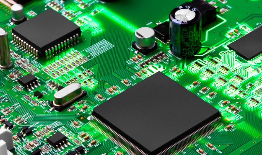
As our global society becomes increasingly concerned about the environment, industries are rethinking how they operateincluding the electronics sector. At the heart of nearly all electronic devices lies the PCB Prototype, or Printed Circuit Board prototype, which serves as the essential backbone for electrical connectivity. Traditionally, PCB manufacturing has not been environmentally friendly. Toxic chemicals, energy-intensive production, and non-recyclable materials have raised major concerns.
However, a new wave of innovation is steering this crucial industry toward a more sustainable future. The rise of eco-friendly PCB prototypes represents a pivotal shift toward environmental responsibility, focusing on sustainable materials, recyclable components, and energy-efficient manufacturing. In this article, well explore how these advancements are influencing the electronics landscape and what it means for consumers and manufacturers alike.
Understanding the Environmental Impact of Traditional PCBs
Before we dive into sustainable alternatives, it's essential to understand the environmental challenges posed by traditional PCB production. Standard PCBs typically use FR-4 substrate, a glass-reinforced epoxy laminate thats not biodegradable and is hard to recycle. Manufacturing these boards often involves:
- Hazardous chemicals such as lead, brominated flame retardants, and volatile organic compounds (VOCs).
- Energy-intensive processes like etching, plating, and curing.
- Waste management issues, including toxic sludge and electronic waste (e-waste).
These processes contribute significantly to air, water, and soil pollution while also generating large amounts of industrial waste. As electronic device usage skyrockets globally, so does the ecological footprint of PCB production.
If youre curious to Find Out More about these processes and their impact, numerous whitepapers and environmental reports detail how traditional electronics contribute to pollution. But the good news is, change is already underway.
The Rise of Eco-Friendly PCB Prototypes
Sustainability is no longer a buzzwordits a business imperative. As environmental regulations tighten and consumers demand greener products, PCB manufacturers are investing in eco-friendly materials and green technologies. Here's how the industry is evolving:
1. Bio-based and Recyclable Substrates
One of the most revolutionary shifts in PCB prototyping is the use of biodegradable and recyclable substrates. Researchers and startups are experimenting with:
- Natural fiber composites: Materials like jute, flax, and hemp are being combined with resins to create durable yet biodegradable boards.
- Paper-based PCBs: While still in early stages, some low-power electronics are already being tested with paper as a core substrate.
- Recyclable thermoplastics: Unlike thermoset plastics, which cant be remelted, recyclable thermoplastics allow for easier material recovery and reuse.
These materials drastically reduce the environmental footprint, especially during the end-of-life phase of electronic products. Check over here for case studies on how companies are implementing these materials in real-world applications.
2. Lead-Free and RoHS-Compliant Soldering
The Restriction of Hazardous Substances (RoHS) directive in the European Union prohibits the use of dangerous materials such as lead, mercury, and cadmium in electronics. Consequently, lead-free soldering has become the norm for eco-friendly PCB prototypes.
This shift not only aligns with legal compliance but also improves worker safety and reduces soil and water contamination. Modern soldering alloys use tin, silver, and copper instead of toxic heavy metals, maintaining performance while ensuring environmental safety.
3. Green Manufacturing Processes
Beyond materials, manufacturers are investing in clean and energy-efficient production methods to minimize waste and emissions. Some innovations include:
- Closed-loop water systems to recycle water during PCB etching and cleaning.
- Dry etching techniques that use plasma instead of chemicals.
- Low-temperature curing resins, which reduce energy consumption.
- Digital fabrication methods, such as 3D printing PCBs, which minimize waste.
Companies that focus on these processes not only reduce their carbon footprint but also benefit from long-term cost savings and enhanced corporate responsibility branding.
If youre a manufacturer looking to implement green practices, go right here to access guides and toolkits that outline how to make your facility more eco-friendly.
Benefits of Sustainable PCB Prototypes
The push for sustainability in PCB prototyping isn't just about compliance or reputationits also about long-term economic and environmental gains. Here are a few of the major benefits:
Environmental Protection
- Reduction of toxic waste in landfills.
- Lower greenhouse gas emissions during production.
- Preservation of natural resources through recycling and material reuse.
Improved Corporate Responsibility
Green practices are a key part of ESG (Environmental, Social, and Governance) reporting. Companies that adopt sustainable PCBs can demonstrate responsibility to stakeholders, gaining a competitive edge in both B2B and consumer markets.
Better Product Lifecycle Management
Eco-friendly PCBs can often be disassembled and recycled more easily, making it easier to comply with take-back regulations and e-waste management programs.
Challenges and Barriers to Adoption
While the benefits are compelling, there are still hurdles in the widespread adoption of eco-friendly PCB prototypes:
- Higher upfront costs: Sustainable materials and green processes can be more expensive initially, although costs tend to decrease over time with scale.
- Limited availability: Not all regions have access to advanced green PCB technologies.
- Technical limitations: Some biodegradable materials may not yet match the durability or conductivity of traditional substrates, especially in high-performance applications.
- Lack of awareness: Many small- to mid-size companies are still unaware of eco-friendly options or how to implement them effectively.
That said, these barriers are steadily falling thanks to increased investment, consumer pressure, and technological breakthroughs. To Find Out More about how businesses are overcoming these challenges, you can explore sustainability case studies from electronics manufacturers whove successfully gone green.
Looking Ahead: The Future of Sustainable Electronics
The future of eco-friendly PCB prototypes is promising. With ongoing research in nanomaterials, biodegradable polymers, and AI-powered waste reduction, sustainable PCB production is poised for mainstream adoption. Key trends to watch include:
- Flexible biodegradable electronics: Perfect for wearables and medical devices.
- Localized manufacturing: Reduces shipping emissions and fosters circular economies.
- Blockchain in supply chains: Offers transparent tracking of materials for sustainable certification.
As more organizations prioritize sustainability, eco-friendly PCBs will no longer be a niche product but a standard expectation.
Conclusion
Eco-friendly PCB prototypes are no longer a futuristic conceptthey're a necessary step toward building a sustainable tech industry. By shifting to bio-based materials, lead-free processes, and green manufacturing techniques, companies can significantly reduce their environmental impact while reaping economic and reputational benefits.
Whether you're a designer, engineer, or manufacturer, the time to act is now. Embrace the future of electronics by exploring sustainable options for your next PCB prototype. If youre ready to dive deeper, check over here for resources, materials, and suppliers leading the green electronics movement.
And if youre still not sure where to begin, go right here to find sustainability audits, certifications, and step-by-step guides tailored for PCB production.